🔑 Key Takeaways
- Coherent secured a $50M CHIPS Act grant to expand its Sherman, Texas facility.
- The fab is the world’s first to produce 6-inch Indium Phosphide (InP) wafers at volume.
- Moving to 6-inch wafers quadruples output and slashes optical die costs by over 60%.
- NVIDIA’s $2B strategic investment ensures priority access to these critical optical components.
- Copper networking fails at the scale of NVIDIA’s 576-GPU NVL576 architecture, mandating photonics.
Artificial intelligence is no longer constrained by how fast a processor can calculate; it is constrained by how fast data can travel between processors. On June 16, 2026, the physical landscape of that data transit shifted fundamentally. Coherent Corp. officially broke ground on a massive expansion of its Sherman, Texas, semiconductor manufacturing facility, backed by a $50 million CHIPS and Science Act grant and a staggering $2 billion strategic investment from NVIDIA. By scaling the world’s first high-volume 6-inch Indium Phosphide (InP) wafer fab, Coherent is actively forging AI’s optical backbone.
With NVIDIA CEO Jensen Huang and Coherent CEO Jim Anderson presiding over the ceremony, the message to the enterprise IT sector was unequivocal: the era of copper networking in the high-performance data center is drawing to a close. As hyperscalers race to build out a Total Addressable Market (TAM) that Bank of America now projects will reach $1.7 trillion by 2030, the connective tissue of these facilities has become the ultimate bottleneck. This expansion in Texas is not just a manufacturing milestone; it is a critical geopolitical and architectural pivot designed to ensure that the speed of light remains a domestic commodity.
The Architectural Reality of AI’s Optical Backbone

To understand why a facility an hour north of Dallas is dictating the future of global computing, one must look at the physical limitations of modern AI infrastructure. The current pinnacle of enterprise AI hardware is the NVIDIA Vera Rubin Ultra NVL576. This architecture does not operate as a single rack; it links eight NVLink racks containing 72 NVIDIA Rubin Ultra GPUs each into a single, unified 576-GPU domain.
When you attempt to span eight racks with traditional copper wiring, physics becomes an insurmountable enemy. At the extreme signaling rates required by modern GPUs, the reach of a metal trace shrinks drastically. Copper suffers from severe signal attenuation over distance. To force a signal across hundreds of feet of copper wire, engineers must deploy arrays of power-hungry retimers and signal conditioners. In a data center environment where power is the most precious and strictly allocated resource, burning megawatts on signal conditioning is an architectural failure.
The only viable solution is silicon photonics. “Optics pays a one-time penalty to move from electrical to light, but once paid, distance is nearly free,” explained Jensen Huang during the groundbreaking. By converting the electrical signals generated by the GPUs into pulses of light, data can travel across the massive expanse of a hyperscale data center with near-zero latency and minimal power degradation. At the NVL576 scale, light is no longer a luxury—it is the most power-efficient, and frankly the only, option available to engineers.
The Physics of Indium Phosphide and the 6-Inch Revolution
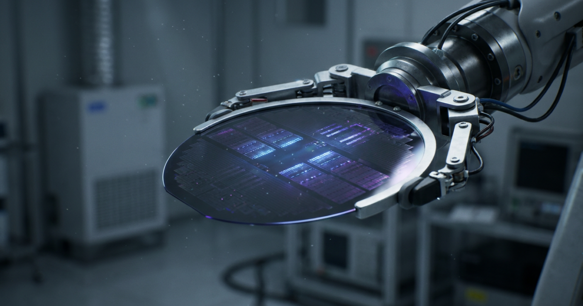
The magic behind this optical conversion does not happen on standard silicon. Silicon is an indirect bandgap semiconductor; it is excellent for logic and compute, but it is notoriously terrible at emitting light. To generate the precise laser pulses required for fiber-optic transmission, the industry relies on III-V compound semiconductors, specifically Indium Phosphide (InP) and Gallium Arsenide (GaAs).
Inside Coherent’s Sherman facility, engineers grow exotic compound-semiconductor layers on InP substrates, tuning them at the atomic level for precise optical properties. These wafers are eventually diced into Electro-absorption Modulated Lasers (EMLs) and Vertical Cavity Surface Emitting Lasers (VCSELs). These microscopic lasers are the beating heart of the pluggable optical transceivers—devices roughly the size of a USB stick—that plug into the front of NVIDIA networking switches.
The true breakthrough of the Sherman facility expansion is not just the material, but the scale. Historically, the global supply chain for InP has been stuck on 3-inch and 4-inch wafers. In the semiconductor world, area scales with the square of the diameter. Moving from a 3-inch wafer to a 6-inch wafer does not double the usable area; it roughly quadruples it. When factoring in the edge exclusion zones where defects are most common, the yield improvements are even more dramatic.
By successfully scaling to a 6-inch InP production line, Coherent is driving down the cost of individual optical dies by more than 60%. This unlocks the massive volume that the AI buildout demands, transforming a bespoke, low-yield manufacturing process into a commoditized, high-volume engine for global connectivity.
Market Impact & Deployment: The $2 Billion NVIDIA Hedge

The financial markets and enterprise stakeholders have not ignored the critical nature of this technology. Coherent’s stock (NYSE: COHR) has surged over 400% in the past year, driven by trailing twelve-month revenues of $6.6 billion and an 18% year-over-year growth rate. But the most telling financial metric is NVIDIA’s direct involvement.
In March 2026, NVIDIA deepened a two-decade relationship with Coherent by injecting $2 billion into the company. This strategic investment was earmarked specifically to support R&D, future capacity, and U.S.-based manufacturing, alongside a multibillion-dollar purchase commitment for advanced laser and optical interconnects. NVIDIA is effectively hedging its entire hardware roadmap. They recognize that producing the world’s fastest GPUs is irrelevant if they cannot source the optical transceivers required to network them together.
Furthermore, the geopolitical implications of the Sherman facility cannot be overstated. The $50 million CHIPS Act grant, combined with $17 million from the Texas Semiconductor Innovation Fund and local Sherman economic grants, represents a concerted federal and state effort to onshore critical supply chains. While logic chips (like CPUs and GPUs) dominate the headlines, the domestic supply chains for compound semiconductors have been dangerously thin for years, heavily reliant on Asian manufacturing and packaging. The Sherman expansion, which will create over 1,000 new jobs (including 550 direct advanced manufacturing roles), is a concrete step toward securing U.S. sovereignty over the entire AI hardware stack.
The Consumer Translation: Beyond the Data Center
For the average consumer, the physics of Indium Phosphide and the geometry of 6-inch wafers may seem entirely abstracted from daily life. However, the downstream effects of this manufacturing leap will be profound and ubiquitous.
Think of a data center’s internal network like a country’s logistics infrastructure. Copper wiring is the equivalent of a fleet of local delivery trucks—highly effective for short, neighborhood routes, but disastrously inefficient and expensive for cross-country freight. Optical interconnects are the high-speed rail network. By drastically lowering the cost and increasing the availability of this “high-speed rail,” Coherent is fundamentally lowering the cost of computing.
When hyperscalers spend less money on power and networking hardware, the cost to train and run massive Large Language Models (LLMs) drops. This translates directly into cheaper, more capable AI agents for consumers. It means real-time, zero-latency voice translation on smartphones. It accelerates computational fluid dynamics for safer automotive designs, and it supercharges the protein folding algorithms that drive modern drug discovery. Furthermore, the commoditization of InP lasers will bleed into other industries, lowering the cost of LiDAR systems for autonomous vehicles and expanding the bandwidth of 6G telecommunications networks.
Frequently Asked Questions
Q1: What is Indium Phosphide (InP) and why is it important for AI?
A1: Indium Phosphide is a compound semiconductor material essential for creating the lasers that power fiber-optic data transmission. Unlike standard silicon, InP can efficiently emit and modulate light, making it the foundational material for the optical transceivers that connect massive AI GPU clusters.
Q2: Why are data centers moving away from copper wiring?
A2: As AI clusters scale to systems like the NVIDIA NVL576 (spanning 8 racks and 576 GPUs), copper wiring suffers from severe signal degradation. Pushing data through copper over these distances requires power-hungry retimers, wasting electricity that hyperscalers would rather dedicate to actual compute processing.
Q3: What is the economic impact of moving to 6-inch InP wafers?
A3: Historically, InP lasers were manufactured on 3-inch or 4-inch wafers. Coherent’s shift to 6-inch wafers quadruples the usable surface area per run. This massive increase in manufacturing efficiency reduces the cost of individual laser dies by more than 60%, significantly lowering the Total Cost of Ownership for AI data centers.
Q4: How does the CHIPS Act factor into this expansion?
A4: Coherent received a $50 million grant from the federal CHIPS and Science Act, supplementing $17 million in local Texas grants. This funding is designed to onshore critical semiconductor manufacturing, reducing U.S. reliance on foreign supply chains for the optical components that wire modern AI infrastructure together.
TechNode HQ Verdict: Pros, Cons & Usability
- Pro (Engineering): The transition to 6-inch InP wafers provides a 4x increase in usable area, slashing die costs by over 60% and solving the critical interconnect bottleneck for 500+ GPU clusters.
- Pro (Consumer): Lowering the Total Cost of Ownership for hyperscale data centers directly accelerates the development and reduces the subscription costs of next-generation consumer AI applications.
- Con: While the wafer fabrication is now secured domestically in Texas, the global supply chain still relies heavily on overseas Outsourced Semiconductor Assembly and Test (OSAT) facilities for final transceiver packaging.
- Con: The upfront capital expenditure required to transition a data center from copper to full silicon photonics remains astronomically high, limiting this architecture to Tier-1 hyperscalers in the near term.
Enterprise Usability: For CTOs and infrastructure architects at the hyperscale or large-enterprise level, the mandate is clear: copper is a dead end for multi-rack AI training clusters. Infrastructure planning for 2027 and beyond must assume a fully optical backbone. Enterprises should audit their current vendor lock-in regarding pluggable optics and prepare for the integration of co-packaged optics (CPO) as switch bandwidths exceed 51.2 Tbps.
Everyday Usability: Consumers cannot buy this technology directly, but they should view this development as the engine that will make localized, high-speed AI agents a reality. As the cost of compute and data transit drops, expect a surge in highly complex, real-time AI services integrated into everyday mobile and smart home devices over the next 24 to 36 months.


