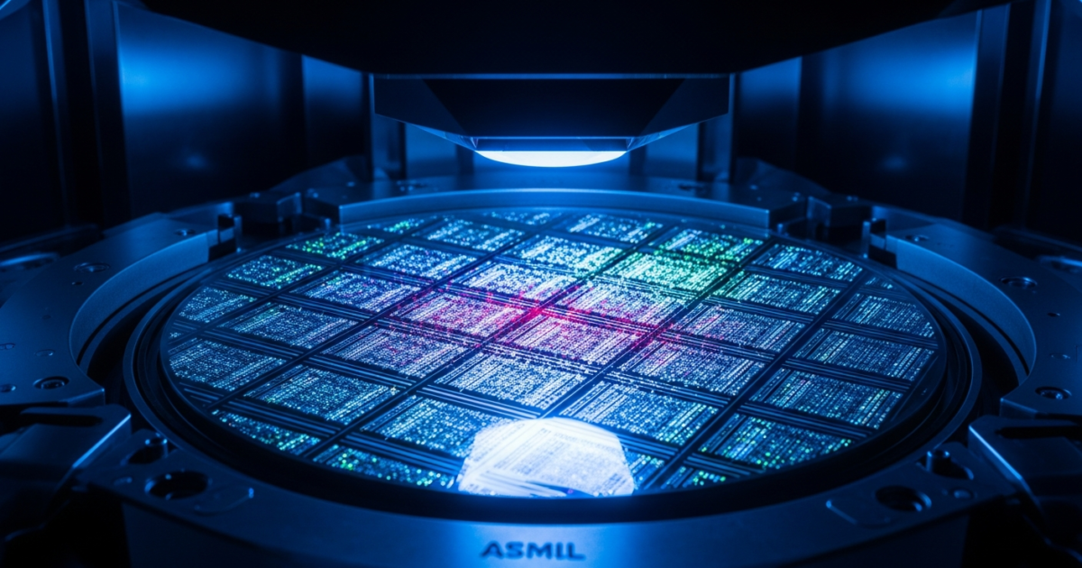
The race toward commercial quantum computing has long been characterized by exotic physics experiments, cryogenic chandeliers, and bespoke fabrication ecosystems that look nothing like the traditional semiconductor industry. However, a watershed announcement from Belgian semiconductor research giant Imec has fundamentally altered this trajectory. Unveiled at ITF World in Leuven on May 19, 2026, Imec has successfully fabricated the world’s first quantum dot qubit device using High-NA EUV lithography.
This is not merely another incremental physics milestone. By patterning silicon quantum dot spin qubits at gate gaps of barely 6 nanometers using the exact same $400 million ASML lithography machines destined to print the next generation of AI accelerators, Imec has proven that quantum computing can piggyback on the existing, multi-trillion-dollar CMOS manufacturing roadmap. The implications for compressing the timeline toward commercially viable quantum systems are profound, shifting the industry’s primary bottleneck from theoretical physics to industrial-scale manufacturing.
The Architectural Reality

To understand the magnitude of Imec’s breakthrough, one must dissect the underlying architecture of both the manufacturing tool and the quantum hardware it produces. For the past decade, the quantum computing industry has been fragmented across various qubit modalities: superconducting loops (championed by IBM and Google), trapped ions (IonQ and Quantinuum), and photonic systems (PsiQuantum). While these architectures have successfully demonstrated quantum supremacy in isolated laboratory settings, they all suffer from a fatal flaw: they are notoriously difficult to scale to the millions of qubits required for fault-tolerant quantum computers.
Enter quantum dot spin qubits. Often referred to as “industry qubits,” these nanoscale structures are built using silicon—the very same material that has powered the digital revolution for the last sixty years. These qubits operate by trapping individual electrons inside microscopic silicon structures. The quantum “spin” state of the trapped electron (up, down, or a superposition of both) is utilized to store and process quantum information. Surrounding metallic control gates, known as plunger and barrier gates, are used to manipulate the interactions between neighboring quantum dots.
While the concept is elegant, the fabrication is exponentially complex. The performance, controllability, and interaction fidelity of quantum dot spin qubits depend entirely on the physical spacing between these control electrodes. As neighboring quantum dots are moved closer together, their coupling strength rises exponentially. To achieve the fidelity required for fault-tolerant quantum operations, these gaps must be patterned at a scale of just a few nanometers, consistently, across an entire 300mm silicon wafer. Until now, this level of precision at an industrial scale was physically impossible.
Imec solved this by deploying High-NA EUV (High Numerical Aperture Extreme Ultraviolet) lithography. Developed by Dutch monopoly ASML, High-NA EUV represents the pinnacle of human engineering. By increasing the optical system’s numerical aperture from 0.33 to 0.55, the technology allows for dramatically smaller and more accurate features to be printed onto silicon wafers. The machine itself is a behemoth: it weighs over 150 tons, spans the length of a double-decker bus, and requires an entirely redesigned optical system with mirrors polished by ZEISS to atomic precision.
Using this cutting-edge tool—which Imec only received in its 300mm cleanroom in March 2026—researchers were able to pattern functioning qubit arrays with gaps of barely 6 nanometers. This is a staggering achievement. It proves that the semiconductor industry’s most advanced manufacturing tool, originally designed for sub-2nm CPUs and AI GPUs, can be directly applied to quantum hardware. It effectively moves silicon spin qubits out of the bespoke laboratory environment and into the realm of standardized, high-volume chip manufacturing.
The Manufacturing Bottleneck and CMOS Compatibility
The central problem facing quantum computing today is no longer whether researchers can create functioning quantum systems; it is whether they can manufacture them at scale. A commercially useful quantum computer capable of breaking RSA encryption or simulating complex molecular structures will require millions of physical qubits to achieve a sufficient number of logical, error-corrected qubits.
Building a machine with millions of superconducting qubits would require cryogenic refrigerators the size of football stadiums and a wiring complexity that defies current engineering capabilities. Silicon quantum dot spin qubits, however, offer a distinct advantage: they are microscopic, and their production process is largely compatible with standard CMOS (Complementary Metal-Oxide-Semiconductor) manufacturing.
By demonstrating that High-NA EUV can pattern these qubits, Imec has shown that the quantum industry does not need to invent a new manufacturing paradigm from scratch. Instead, it can leverage the $500 billion global semiconductor supply chain. Decades of transistor scaling, wafer handling, defect mitigation, and metrology expertise can now be directly applied to quantum hardware. This convergence means that as foundries like TSMC, Intel, and Samsung invest billions in High-NA EUV to build the next generation of AI accelerators, they are simultaneously laying the groundwork for industrial-scale quantum computer manufacturing.
Market Impact & Deployment

The market implications of Imec’s announcement are seismic, but they must be viewed through the lens of extreme capital expenditure. High-NA EUV is not a democratized technology. Each ASML Twinscan EXE system costs between $350 million and $400 million. The infrastructure required to house them—massive cleanrooms with specialized vibration isolation and power delivery—adds hundreds of millions more to the total cost of ownership (TCO).
Currently, only a handful of companies on Earth can afford to deploy this technology. Intel was the first to install a commercial High-NA EUV tool late in 2023 to support its 14A process node. TSMC, the world’s largest contract chipmaker, has publicly expressed hesitation regarding the exorbitant sticker price of High-NA EUV, stating that their existing Low-NA EUV tools combined with multi-patterning techniques may suffice for their immediate roadmap. However, Imec’s demonstration that High-NA EUV is essential for 6nm quantum gate gaps may force foundries to accelerate their adoption timelines if they wish to capture the future quantum foundry market.
For enterprise IT leaders and CTOs, this development signals a shift in how quantum computing will be commercialized. The convergence of quantum hardware with CMOS manufacturing means that traditional semiconductor giants (Intel, Samsung, TSMC) are uniquely positioned to dominate the quantum hardware space, potentially displacing pure-play quantum startups that rely on exotic, non-scalable architectures.
Furthermore, this reinforces the reality that quantum computing will be strictly a cloud-based enterprise service. The sheer cost of the manufacturing equipment, combined with the cryogenic cooling required to operate silicon spin qubits (which still need to be cooled to near absolute zero to maintain quantum coherence), guarantees that these machines will be housed in centralized hyperscaler data centers. Enterprises will access this computational power via AWS, Google Cloud, or Microsoft Azure, integrating quantum processing units (QPUs) alongside traditional CPUs and AI GPUs to tackle specific, highly complex workloads.
The Consumer Translation
For the everyday consumer, the phrase “High-NA EUV-fabricated quantum dot qubit device” sounds like science fiction jargon. It is vital to understand that consumers will never hold a quantum computer in their hands. There will be no “Quantum iPhone” or “Quantum PlayStation.” The physics of maintaining quantum states requires extreme isolation from heat, electromagnetic interference, and even cosmic rays.
However, the downstream impact of Imec’s breakthrough on the public will be transformative. By accelerating the timeline to fault-tolerant quantum computing, we are accelerating the timeline to the solutions these machines will provide.
Classical supercomputers, no matter how powerful, are fundamentally limited when it comes to simulating nature. Simulating the exact behavior of a complex molecule for drug discovery currently requires massive approximations. A scaled quantum computer, utilizing the silicon spin qubits Imec is pioneering, could simulate molecular interactions with perfect accuracy. This translates directly to the rapid discovery of targeted pharmaceuticals, personalized medicine, and cures for currently untreatable diseases.
Beyond healthcare, consumers will feel the impact in the physical products they use. Quantum computers will enable the discovery of new, lightweight, hyper-conductive materials for solid-state EV batteries, potentially extending electric vehicle ranges by hundreds of miles. They will optimize global logistics and supply chains, reducing shipping costs and carbon emissions. They will also force a complete overhaul of global cybersecurity, as quantum algorithms will easily crack current encryption standards, ushering in an era of quantum-safe cryptography that will secure consumer banking and private communications.
TechNode HQ Verdict: Pros, Cons & Usability
- Pro (Engineering): Achieves unprecedented 6nm gate gaps for silicon spin qubits using industry-standard High-NA EUV, exponentially increasing coupling strength and interaction fidelity while proving CMOS compatibility.
- Pro (Consumer): Accelerates the timeline for commercial quantum applications, bringing society closer to breakthroughs in molecular simulation, drug discovery, and next-generation battery materials.
- Con: The staggering $400 million cost per High-NA EUV machine creates an insurmountable barrier to entry, consolidating future quantum manufacturing power into the hands of just three or four global foundries.
- Con: While manufacturing scaling is addressed, the announcement glosses over the massive engineering hurdles of cryogenic control wiring, error correction overhead, and qubit yield rates across a 300mm wafer.
Enterprise Usability: For CTOs and Enterprise IT architects, this is a strong signal to begin quantum-readiness auditing. While you will not buy this hardware, you will rent it. Enterprises should actively invest in quantum-safe cryptography transitions today and begin upskilling data science teams on quantum algorithms via cloud-based simulators. The hardware roadmap is now aligning with traditional semiconductor timelines, meaning the leap from prototype to commercial cloud availability could happen faster than previously modeled.
Everyday Usability: The public should not expect any immediate changes to their consumer electronics. This is deep-tech infrastructure. However, consumers should be aware that the AI boom currently dominating headlines is merely the precursor. The same manufacturing technology printing today’s AI chips is now printing tomorrow’s quantum processors, setting the stage for a computational revolution that will redefine healthcare, energy, and digital security over the next decade.
Sources & Citations:
Original Claim via: tomshardware [3]
Official Handle: @tomshardware
Topics Explored: High-NA EUV, Quantum Computing, Imec, Silicon Qubits, ASML


