Key takeaways
- Terafab targets initial machinery commissioning in early 2027 and a first test chip by May or June 2027.
- High-volume manufacturing is planned for late 2028 across sites in Austin and Grimes County, Texas.
- Capital equipment expenditures are expected to reach tens of billions by 2028 and may surpass $100 billion long-term.
- Industry specialists remain skeptical of the timeline given standard multi-year lead times for advanced lithography and cleanroom ramp-up.
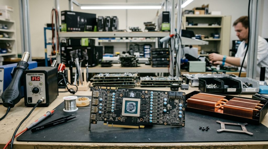
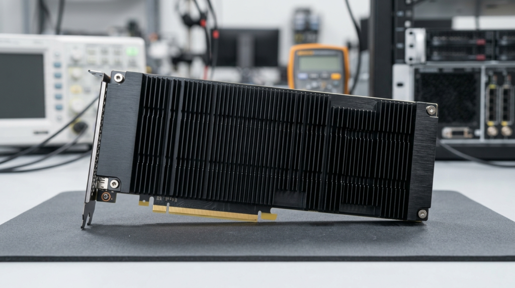
Elon Musk announced that Terafab, a joint semiconductor manufacturing venture between Tesla and SpaceX, aims to begin commissioning machinery in early 2027 and produce its first test chip around May or June 2027. Speaking on Tesla’s third-quarter earnings call, Musk projected that the facility would achieve volume production by late 2028 to supply custom silicon for Tesla’s Optimus humanoid robots and autonomous vehicle fleet. The initiative involves a dual-site strategy in Texas, pairing an initial prototyping line at Giga Texas in Austin with a planned volume production megafacility in Grimes County. Capital investment is expected to exceed tens of billions of dollars by 2028, though semiconductor analysts remain skeptical of the rapid timeline.
Musk’s Terafab timeline and capital commitments
According to reporting from Gizmodo, Musk stated that equipment commissioning would begin in the first half of 2027. He described the goal as an initial proof of viability: “hopefully if things go well, we’ll make our first test chip, just to see if we can make any chip at all, around May or June.” Real commercial production is slated for late 2028, a pace Musk acknowledged as “lightning fast by fab standards.”
The project is structured as a collaboration between Tesla and SpaceX, two companies currently discussing a potential corporate merger. On the earnings call covered by Deccan Chronicle, Musk noted that the companies have yet to determine the formal split of financial responsibilities. He emphasized that capital equipment expenditures would reach tens of billions of dollars through early 2028 and could eventually surpass $100 billion over the long term.
Musk framed the fabrication facility as a prerequisite for scaling physical artificial intelligence systems, calling it “an incredibly important asset, if not a necessary asset,” for the Optimus humanoid robot program. While low-rate manufacturing has begun on a pilot assembly line in Fremont, California, Musk acknowledged that reaching Tesla’s stated target of 20,000 robots weekly will require at least another year. Complex electromechanical challenges surrounding the robotic hands remain unresolved, with Tesla aiming to finalize hand designs by the end of 2027 before delivering units to industrial customers for repetitive tasks.
Dual-site Texas strategy and equipment deliveries
The Terafab initiative encompasses a dual-site operational model in Texas, as documented on Wikipedia. Early research, development, and prototyping lines are being established at Giga Texas in Austin. Meanwhile, large-scale commercial manufacturing is planned for a dedicated complex in Grimes County. A technical overview from Manufacturing Digital indicates the project is designed as a vertically integrated megafacility combining logic fabrication, memory integration, and advanced packaging under one roof to minimize external foundry dependence.
To support this schedule, critical semiconductor manufacturing equipment suppliers, including Dutch lithography vendor ASML, have reportedly agreed to expedite tool deliveries, according to Tom’s Hardware. Terafab is scheduled to receive its first extreme ultraviolet (EUV) lithography tool from ASML in mid-2027 to outfit the Austin experimental line, as reported by Tom’s Hardware.
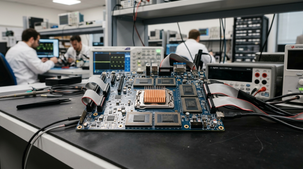
Procuring advanced equipment represents only one component of foundry readiness. Advanced chip research facilities such as the Applied Materials EPIC Center demonstrate that deploying cutting-edge process technology requires extensive co-development across tooling, chemical materials, and metrology before production begins.
| Project Phase | Target Window | Facility Location | Operational Objective |
|---|---|---|---|
| Machinery Commissioning | H1 2027 | Giga Texas (Austin) | Cleanroom tool installation and baseline qualification |
| First Test Silicon | May–June 2027 | Giga Texas (Austin) | Initial experimental test chip using first EUV scanner |
| High-Volume Scaling | Late 2028 | Grimes County, Texas | Commercial wafer production for Optimus and vehicle fleets |
| Full Vertical Integration | Post-2028 | Texas Dual-Site Complex | Unified packaging, memory integration, and logic fabrication |
Semiconductor industry skepticism and cleanroom realities
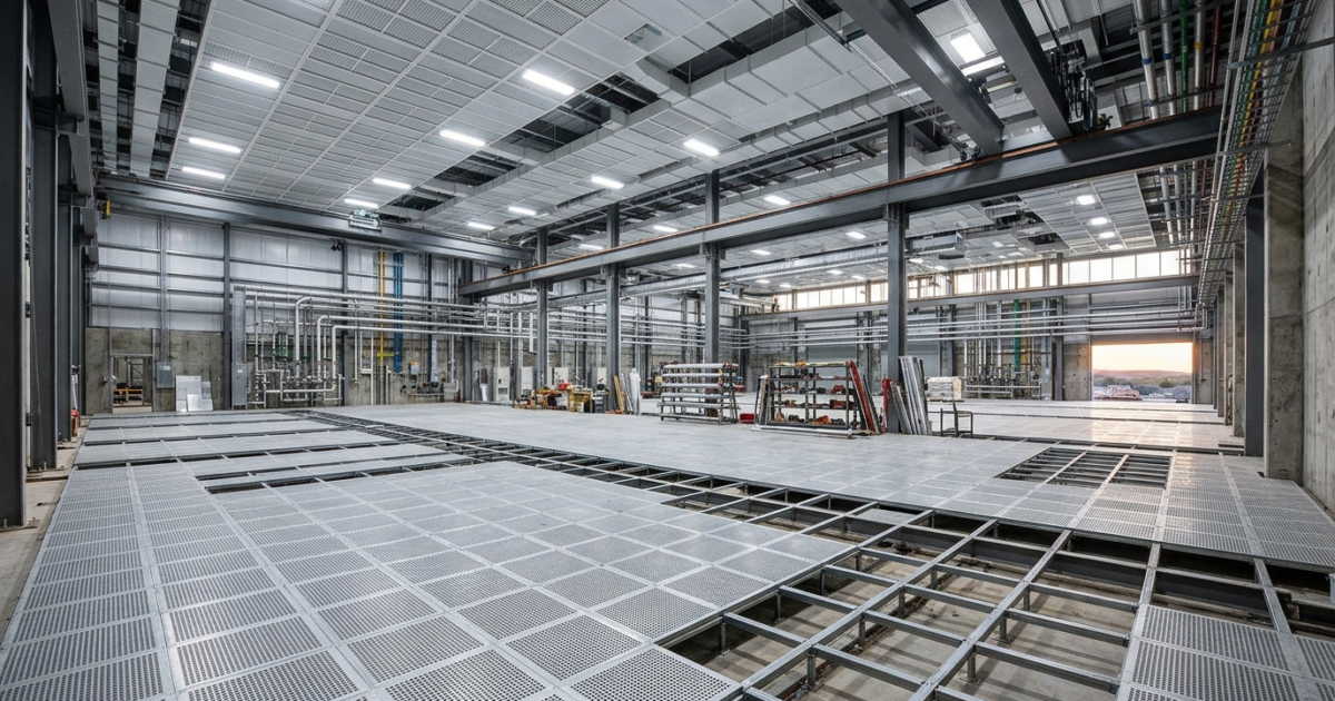
Semiconductor industry analysts cited by The Edge Singapore express deep skepticism regarding Terafab’s 2027 and 2028 projections. Establishing a greenfield semiconductor fab typically requires three to five years under optimal conditions. Construction teams must build vibration-isolated foundations, ultra-clean airflow systems, continuous chemical supply lines, and industrial water-recycling infrastructure before tools can be installed.
Even if ASML delivers an EUV tool on an expedited schedule in mid-2027, installing and calibrating a lithography scanner takes several months of precision engineering. If cleanroom facilities are not certified on time, delicate optical equipment may sit idle in shipping crates. Furthermore, manufacturing a preliminary test chip to verify basic connectivity is distinct from achieving stable commercial yields. Established foundries spend years refining defect density, power profiles, and thermal characteristics across multi-step fabrication recipes before reaching volume production.
What happens next
The immediate operational priority for Terafab involves concluding cost-allocation discussions between Tesla and SpaceX, which remains intertwined with their broader merger evaluation. Observers and infrastructure engineers will monitor construction progress at Giga Texas throughout 2026 to see if physical cleanrooms are ready to accept tooling in early 2027.
At the same time, Tesla must navigate independent technical and regulatory hurdles across its transport portfolio. The automaker plans to begin customer purchases for its two-seater Cybercab by the end of this year and expand transport services to Dallas, while responding to National Highway Traffic Safety Administration inquiries regarding safety self-certifications. Whether Terafab meets its June 2027 test chip milestone will provide the first concrete measure of whether Musk’s internal silicon strategy can match the company’s hardware ambitions.
Sources
- Elon Musk Claims His Terafab Will Produce Its First Chip By Mid-2027
- SpaceX and Tesla’s Terafab Targets 2028 For Volume Chip Production, Says Musk
- Elon Musk says ASML and other critical semiconductor equipment suppliers will expedite shipments to Terafab — facility targets volume chip production by Q3-Q4, 2028, in ‘highly aspirational’ timeline | Tom’s Hardware
- Elon Musk’s Terafab will reportedly receive its first EUV chipmaking tool from ASML in mid-2027 — cutting-edge scanner could sit idle for some time as experimental facility is completed | Tom’s Hardware
- Musk says ASML, others expediting chipmaking gear for Terafab
- How Elon Musk’s Texas Terafab will Make AI Chips | Manufacturing Digital
- Terafab – Wikipedia