
Key takeaways
- Applied Materials invested $5 billion to open the EPIC Center, a 600,000-square-foot collaborative R&D facility in Silicon Valley featuring nearly four acres of cleanroom space.
- The shared operational model co-locates equipment developers with major chipmakers—including TSMC, Intel, Samsung, Micron, and SK hynix—to cut development cycle times by at least 30%.
- Research focuses on post-scaling fabrication challenges, including 3D transistor architectures, low-resistance wiring, hybrid bonding, and heterogeneous packaging.
- The parallel development methodology aims to validate process recipes and materials before equipment reaches production fabs, supporting roadmaps toward trillion-transistor packages by 2030.
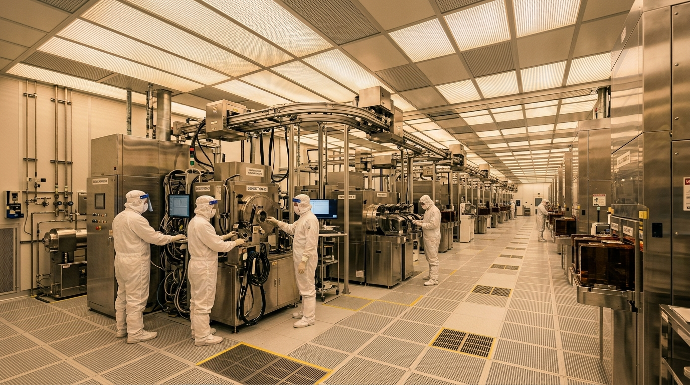
Applied Materials Inc. has officially opened its Equipment and Process Innovation and Commercialization Center, known as the EPIC Center, a $5 billion research and development facility in Silicon Valley. Designed to address severe compute and power bottlenecks created by generative AI infrastructure, the 600,000-square-foot facility provides nearly four acres of cleanroom space where commercial chipmakers and equipment engineers will work side-by-side. The shared facility aims to reduce traditional semiconductor process development cycles by at least 30%, targeting critical bottlenecks across transistor architecture, hybrid bonding, low-resistance wiring, and 3D packaging.
EPIC Center scale and collaborative operating model
Historically, bringing a new semiconductor manufacturing process node from exploratory materials research to commercial high-volume manufacturing has required up to a full decade of iterative development. In traditional fabrication roadmaps, equipment suppliers like Applied Materials develop tooling in relative isolation before shipping prototypes to customer cleanrooms, where chipmakers then identify yield, thermal, and interface defects in sequential cycles. The EPIC Center alters this operational sequence by co-locating customer engineers directly inside Applied Materials’ research infrastructure before tools and process recipes reach production fabs.
According to Applied Materials, the physical facility required massive structural investments to support high-density processing equipment and stringent cleanroom vibration tolerances. The structure houses enough structural steel to build two Eiffel Towers and sits on a foundation containing enough concrete to fill 34 Olympic-sized swimming pools, as reported by the New York Post. Inside, nearly four acres of cleanrooms are configured to run parallel experiments spanning equipment modification, novel chemistry deposition, and process qualification.
| Parameter | Reported specification | Operational significance |
|---|---|---|
| Total capital investment | $5 billion | Directly funded by Applied Materials for construction, infrastructure, and advanced tooling. |
| Facility footprint | Over 600,000 square feet | Combines cleanroom, advanced metrology laboratories, and collaborative workspaces. |
| Cleanroom area | Nearly 4 acres | Houses parallel pilot lines for multi-company process co-optimization. |
| Structural materials | Steel equivalent to 2 Eiffel Towers; concrete for 34 Olympic pools | Constructed to meet rigorous vibration damping and cleanroom isolation standards. |
| Development cycle target | 30% reduction in cycle duration | Vendor projection intended to compress typical 10-year research timelines. |
Dr. Prabu Raja, President of the Semiconductor Products Group at Applied Materials, stated that coordinating equipment, process technology, and material design in parallel is essential because materials at atomic dimensions behave in fundamentally unexpected ways. By allowing customer engineers to optimize interfaces and equipment parameters prior to factory installation, the equipment vendor projects that new tools will arrive at customer fabs capable of faster yield ramps and higher initial performance.
Technical focus areas and foundry coalition
The operational mandate of the EPIC Center reflects the physical limitations confronting classical 2D lithographic scaling. As planar shrink yields diminish, performance gains in high-performance computing rely on complex heterogeneous integration and vertical stacking. Research teams at the facility will concentrate on five to ten critical process domains identified by Applied Materials Chief Executive Gary Dickerson as principal determinants of yield and energy efficiency.
Key architectural and material focus areas inside the facility include:
- 3D architectures: Developing uniform deposition and high-aspect-ratio etching techniques for gate-all-around (GAA) nanosheet transistors and complementary FET (CFET) structures.
- Low-resistance interconnects: Integrating alternative metals and thin barrier layers to lower interconnect resistance and thermal bottlenecks at sub-2nm dimensions.
- Advanced packaging and hybrid bonding: Refining direct copper-to-copper wafer-to-wafer and die-to-wafer bonding to support high-density multi-chiplet integration.
- Atomic-scale interface engineering: Controlling chemical behaviors and surface degradation across heterogeneous material boundaries.
To execute this research, Applied Materials established a coalition of founding partners that encompasses the world’s leading semiconductor manufacturers: Taiwan Semiconductor Manufacturing Co. (TSMC), Intel Corp., Samsung Electronics Co. Ltd., Micron Technology Inc., and SK hynix Inc. The facility also incorporates innovation partners such as Broadcom Inc. and Advantest Corp., alongside academic researchers from Stanford University, UC Berkeley, and UCLA, as noted by EE Times.
Intel Chief Executive Lip-Bu Tan underscored the necessity of this multi-party collaboration, highlighting the industry roadmap toward packaging more than one trillion transistors into a single module by 2030. Achieving this density requires tighter synchronization between equipment vendors, foundries, and packaging specialists to control escalating R&D costs and complex thermal-electrical trade-offs.
What happens next
With cleanroom operations now open, resident engineering teams from founding partners are scheduled to begin joint research projects across advanced packaging and atomic-scale materials. Applied Materials has declined to disclose proprietary details regarding initial client projects, citing customer confidentiality agreements. However, initial process workflows are expected to concentrate heavily on advanced packaging and hybrid bonding interconnects demanded by next-generation accelerators.
For hardware engineers and procurement teams, the facility’s success will be measured by whether the projected 30% cycle-time reduction translates into commercial fab yield timelines before the end of the decade. As chipmakers balance multi-billion-dollar R&D budgets against soaring fab construction costs, the industry will watch whether shared equipment R&D yields scalable process standards without compromising competitive intellectual property boundaries between rival foundries.