Key takeaways
- 4 GHz, identified via Linux kernel microcode as Family 1Ah, Model DCh (Zen 6 architecture).
- Memory configuration includes 24GB of LPDDR5 running at 9,600 MT/s across four 6GB SK Hynix packages, offering a substantial bandwidth increase over current handhelds.
- The “Gainsborough” codename mirrors Valve’s Final Fantasy VII naming tradition (Aerith, Sephiroth), fueling speculation of a next-generation Steam Deck SoC, though neither AMD nor Valve has confirmed commercial production.
An unreleased AMD engineering sample APU featuring next-generation Zen 6 CPU cores and 24GB of high-speed LPDDR5 memory has surfaced on the OpenBenchmarking database. Identified by part number 100-000001930-12_Y and evaluated on an AMD GBR-FF6-SKT validation board, the six-core, 12-thread processor operates at 2.4 GHz alongside memory running at 9,600 MT/s. Associated with the internal codename Gainsborough, the chip has drawn intense interest as a prospective custom silicon candidate for next-generation gaming handhelds, including a potential successor to Valve’s Steam Deck. However, early benchmark runs reflect preliminary validation testing rather than production silicon, and neither AMD nor Valve has confirmed any commercial deployment.
Engineering sample specifications and benchmark findings
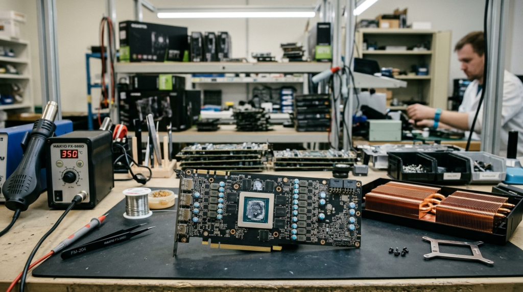
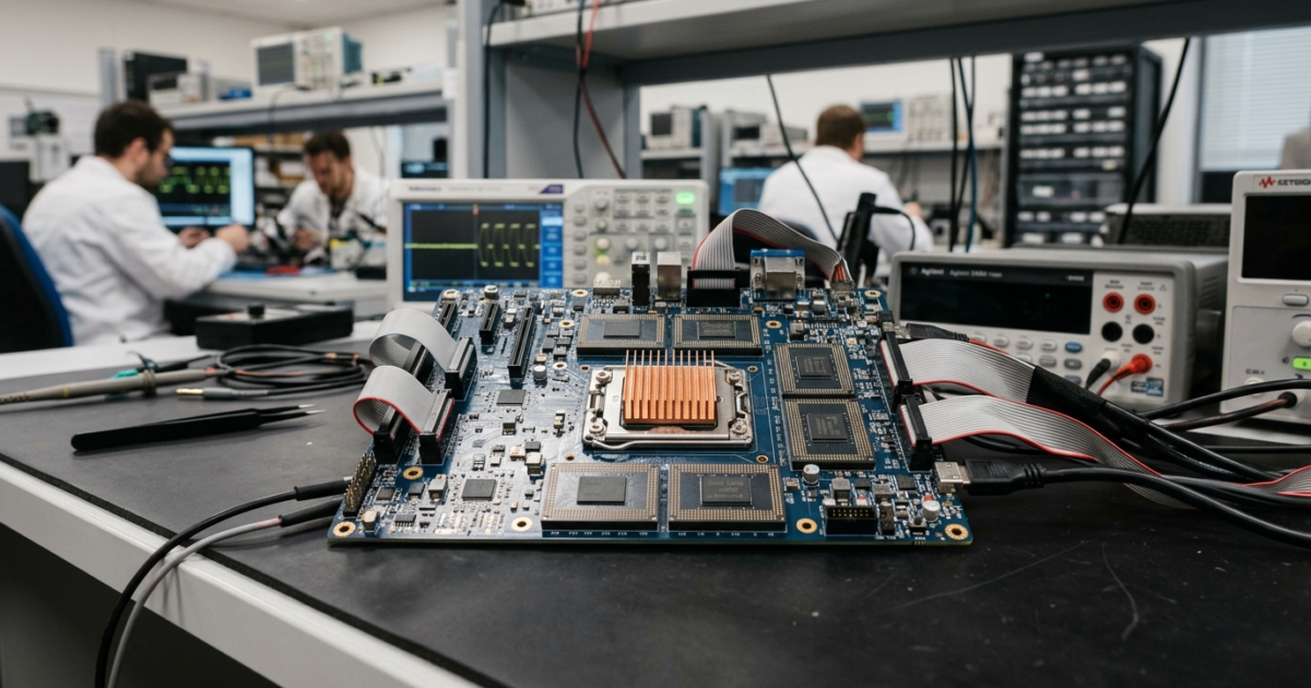
The benchmark entry, first highlighted by TechPowerUp and detailed by Tom’s Hardware, reveals an engineering sample designated 100-000001930-12_Y running on an internal test platform dubbed GBR-FF6-SKT. The system combines an AMD processor configured with six physical cores and 12 simultaneous threads clocked at a flat base frequency of 2.4 GHz. Rather than standard desktop DDR5 modules, the board is populated with four 6GB SK Hynix LPDDR5 packages, delivering a 24GB unified memory pool operating at 9,600 MT/s.
Graphics rendering on the test unit is handled by an integrated GPU clocked at 2,400 MHz. The OpenBenchmarking record documents preliminary runs under Ubuntu 24.04 LTS using early Mesa open-source drivers within the synthetic GpuTest suite at a 1024×768 render target. Recorded figures include 3,508 points in FurMark, 3,871 points in GiMark, and 9,319 points in TessMark. While the raw FurMark score falls in line with the baseline performance of the original Steam Deck, synthetic runs on development boards with unfinalized firmware, locked clocks, and immature graphics drivers do not reflect final gaming frame rates or sustained thermal behavior.
| Hardware Metric | Steam Deck (Aerith / Sephiroth) | AMD Engineering Sample (100-000001930-12_Y) |
|---|---|---|
| CPU Microarchitecture | Zen 2 (4 cores / 8 threads) | Zen 6 (6 cores / 12 threads) |
| Base CPU Clock | 2.4 GHz to 3.5 GHz dynamic | 2.4 GHz (engineering state) |
| Memory Capacity & Type | 16GB LPDDR5 (5,500 to 6,400 MT/s) | 24GB LPDDR5 (9,600 MT/s) |
| Memory Configuration | Four 4GB packages | Four 6GB SK Hynix packages |
| Integrated GPU Clock | Up to 1.6 GHz (8 RDNA 2 CUs) | 2.4 GHz (architecture unconfirmed) |
| Validation Environment | Custom handheld production chassis | AMD GBR-FF6-SKT socketed test board |
Zen 6 microarchitecture and memory bandwidth scaling
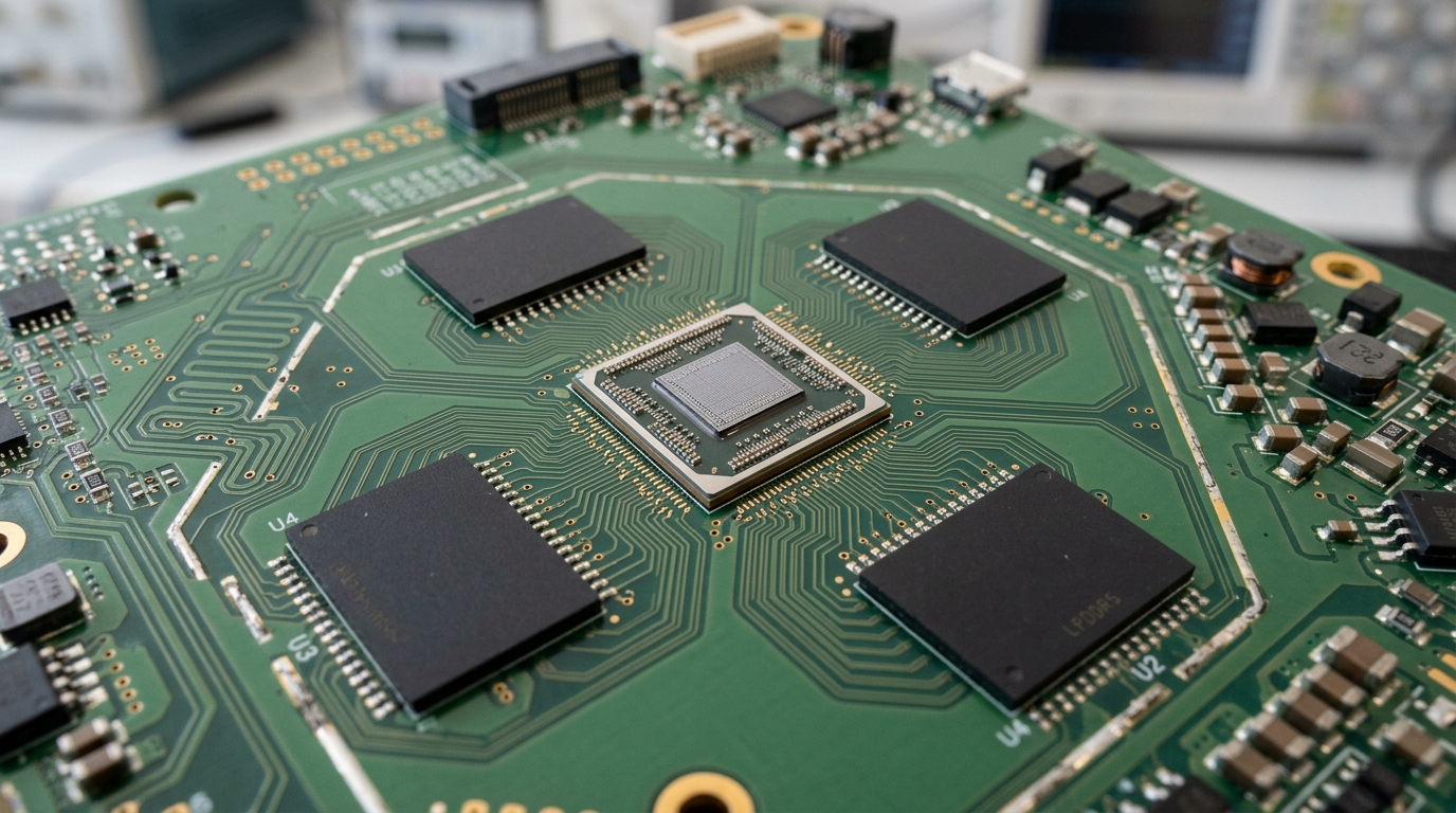
Microcode analysis provides crucial clues regarding the silicon’s lineage. Diagnostic data associates the processor with AMD Family 1Ah, Model DCh. Recent patches to the Linux kernel identify this model range within AMD’s upcoming Zen 6 architecture family. Whether this specific chip deploys standard Zen 6 cores, compact Zen 6c dense cores, or a hybrid topology remains unverified, as early engineering identifiers do not expose core layout particulars.
For compact systems and handheld gaming devices, memory bandwidth represents the primary architectural bottleneck. In unified memory architectures where the CPU and integrated GPU share a single bus, graphics execution frequently starves during complex 3D rasterization. Scaling data rates from the 6,400 MT/s found in the Steam Deck OLED to 9,600 MT/s delivers a 50 percent increase in theoretical memory bandwidth. Concurrently, expanding capacity to 24GB addresses growing VRAM allocation pressures in modern PC game ports, allowing the operating system, game logic, and high-resolution textures to coexist without aggressive paging or asset downsampling.
Handheld gaming implications and the Steam Deck lineage
The codename Gainsborough has triggered widespread industry analysis due to Valve’s established naming patterns. Valve’s custom APUs have historically used character names from Square Enix’s Final Fantasy VII: the original Steam Deck APU was codenamed Aerith, while the 6nm die shrink in the Steam Deck OLED carried the codename Sephiroth. Gainsborough directly corresponds to the family name of Aerith Gainsborough, suggesting that AMD developed this silicon profile with Valve’s hardware specifications in view.
Nevertheless, engineering samples frequently test exploratory platform configurations that may never reach retail distribution. Valve hardware designers Lawrence Yang and Pierre-Loup Griffais have consistently stated that Valve will not release a Steam Deck 2 until silicon achieves a substantial generational improvement in compute efficiency without compromising portable battery life or thermal balance. A six-core Zen 6 APU paired with 24GB of high-speed memory fits the profile of a platform intended to avoid incremental refreshes in favor of a definitive architectural step forward.
What happens next
Hardware teams must validate early silicon through multiple stepping revisions before reaching commercial production. The current GBR-FF6-SKT test board indicates that AMD is running initial socketed platform bring-up to evaluate electrical stability, memory timing margins with SK Hynix 9,600 MT/s packages, and driver compatibility across the Linux graphics stack.
Technical observers and prospective handheld buyers should monitor future Linux kernel pull requests and Mesa driver commits, where AMD routinely submits enablement patches for new GPU IP blocks and power management features. Until Valve or AMD officially announces a commercial partnership, this silicon represents a promising engineering roadmap for next-generation mobile x86 performance rather than an imminent consumer release.