Key takeaways
- billion in 2025 to between $175 billion and $190 billion by 2027, driven by servers requiring eight times more memory capacity than traditional compute nodes.
- Semiconductor architects are taking divergent approaches to overcome the memory wall: Qualcomm is deploying High-Bandwidth Compute (HBC) to bond compute directly with DRAM, while d-Matrix integrates 3D-stacked DRAM into its Raptor silicon.
- Scale-up networking has converged on high-throughput Ethernet switches and SmartNICs, leveraging dynamic routing algorithms to prevent packet collisions across multi-rack inference clusters.
- Enterprise operators are shifting operational evaluation from pure cost-per-token metrics to business value per task and tokens per watt as physical power and thermal constraints cap cluster density.
Datacenter operators and semiconductor manufacturers are overhauling enterprise infrastructure to keep pace with exponential AI inference demands, shifting focus from raw model training horsepower to energy efficiency and memory throughput. At the AI Infra Summit in Santa Clara, engineering leaders from Amazon Web Services, Qualcomm, d-Matrix, Broadcom, and Oracle Cloud Infrastructure demonstrated how memory bottlenecks, networking latencies, and escalating token costs are dictating the next phase of datacenter design. With AI server memory spending projected to surge fivefold by 2027 and token volumes multiplying rapidly, the industry is confronting physical constraints through novel 3D DRAM integration, direct memory-compute bonding, converged Ethernet switching, and heterogeneous CPU-accelerator topologies.
The pivot to inference and heterogeneous compute
Throughout 2025, datacenter capacity additions were dominated by massive clusters of graphics processing units configured for foundation model pre-training. In 2026, enterprise deployments have tilted overwhelmingly toward day-to-day inference, real-time reasoning, and multi-step agentic workflows. This shift fundamentally alters the compute equation: while training prioritizes raw parallel floating-point operations over months, inference demands low-latency token generation, predictable response times, and strict energy budgets.
Serving persistent inference at enterprise scale requires a more balanced, heterogeneous hardware topology rather than monolithic GPU nodes. Central processing units are reclaiming critical roles in managing inference pipelines, executing orchestrations, preparing vector embeddings, and running application logic alongside dedicated accelerators. For hyperscale operators, custom CPU development has become central to delivering favorable token economics.
According to Peter DeSantis, Senior Vice President at Amazon Web Services, the majority of future cloud compute capacity will be dedicated to serving inference workloads. AWS has anchored its efficiency strategy in its Graviton family of 64-bit Arm-based CPUs. In June 2026, AWS introduced general availability for instances powered by its Graviton5 processor, featuring 192 cores and support for DDR5-8800 memory to handle real-time reasoning and multi-step task orchestration without forcing every operational instruction onto power-dense accelerator silicon. By decoupling orchestration tasks from specialized accelerators, infrastructure operators can significantly lower the overall cost of ownership per completed user request.
Breaching the memory wall: HBC versus 3D DRAM
While compute logic execution continues to advance, memory architecture represents the most acute operational bottleneck in AI infrastructure. SiliconANGLE market data indicates that a typical AI server consumes approximately eight times more memory capacity than an equivalent general-purpose enterprise server. As large models require vast memory pools to maintain model weights and rapidly expanding key-value (KV) caches, total datacenter memory spending is forecast to jump from $35 billion in 2025 to between $175 billion and $190 billion by 2027.
The industry’s central technical impediment remains the classic memory wall—the growing disparity between processing speeds and the speed, capacity, and energy efficiency of data retrieval. At the summit, semiconductor vendors outlined divergent hardware architectures designed to bring compute and storage into tighter physical proximity.
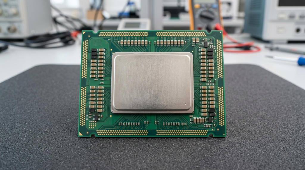
Qualcomm has prioritized an alternative to standard High-Bandwidth Memory (HBM) known as High-Bandwidth Compute (HBC). Traditional HBM relies on 2.5D interposers to connect memory stacks horizontally to compute silicon, a layout that still requires substantial energy to drive signals across interposer traces. Qualcomm’s HBC implements a 3D-stacked silicon approach, bonding compute circuitry directly to DRAM dies.
Tony Pialis, Executive Vice President and General Manager of Datacenter and AI at Qualcomm, highlighted that data movement, rather than mathematical computation, is the primary constraint on modern workloads. Qualcomm estimates that HBC delivers six times the memory bandwidth per watt compared to HBM for large batch inference sizes, and up to 200 times the capacity per watt compared to on-chip Static Random-Access Memory (SRAM). By physically stacking memory and execution units into the same package footprint, data transit distances are shortened from millimeters to micrometers.
| Architecture | Physical Implementation | Primary Efficiency Mechanism | Target Deployment Profile |
|---|---|---|---|
| High-Bandwidth Memory (HBM3e / HBM4) | 2.5D silicon interposer with vertically stacked DRAM dies | High pin-count parallel bus with microbump interconnects | Hyperscale model training and high-concurrency batch inference |
| High-Bandwidth Compute (Qualcomm HBC) | 3D-stacked silicon bonding compute logic directly onto DRAM | Extreme reduction in physical data transit distance to curb routing energy | High-efficiency server inference optimized for tokens per watt |
| 3D DRAM Raptor (d-Matrix) | Multi-layer vertical DRAM cell integration with digital in-memory compute | High-density vertical storage with high internal data throughput | Ultra-low-latency real-time inference and neocloud token services |
| General-Purpose Cloud CPU (AWS Graviton5) | Monolithic Armv9 core array paired with multi-channel DDR5-8800 | Optimized instruction pipeline for branching code and agent orchestration | Pre-processing, embedding retrieval, and multi-step inference coordination |
Conversely, computing startup d-Matrix has pursued memory density through high-throughput 3D DRAM within its Raptor chip architecture. Rather than relying solely on SRAM or standard external DRAM packages, Raptor stacks layers of DRAM cells vertically to maximize capacity directly on the accelerator substrate. Sid Sheth, founder and CEO of d-Matrix, noted during his summit presentation that the vertical stacking approach bypasses SRAM capacity limits while avoiding the supply-chain bottlenecks and thermal complexities of external HBM modules, providing an architecture tailored for continuous token streaming.
Rack-level integration and NVLink Fusion
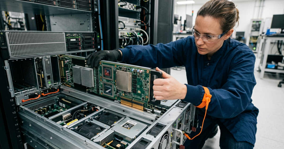
Individual accelerator innovation cannot scale without mechanical and electrical standardization at the server rack level. Power delivery requirements now exceed 100 kilowatts per rack in state-of-the-art configurations, requiring direct-to-chip liquid cooling loops and unified scale-up fabrics. Chip startups face steep hurdles in designing proprietary rack-scale enclosures that enterprise datacenters can deploy reliably.
To overcome deployment friction, d-Matrix unveiled a multi-year partnership with Nvidia to integrate Raptor accelerators directly into Nvidia’s modular rack ecosystem via NVLink Fusion. By aligning with Nvidia’s MGX reference architecture, d-Matrix allows neoclouds, hyperscalers, and enterprise labs to drop third-party inference silicon directly into validated server frames containing NVLink switches, ConnectX networking, and liquid cooling infrastructure. This strategy transforms standard rack enclosures—such as those designed for Nvidia’s Vera architecture—into hybrid configurations capable of running specialized low-latency token pipelines alongside mainstream accelerators.
As power density escalates, industry collaborations like the flexible data center alliance formed by Nvidia, Google, and Emerald AI reflect broader efforts to adapt physical facility designs to high-density compute clusters without triggering thermal runaway or stranded electrical capacity.
Networking fabrics: SmartNICs and lossless Ethernet
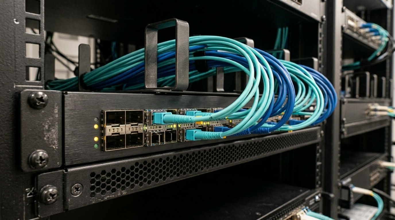
Scaling inference across multi-node configurations shifts operational dependencies toward the datacenter network. A delay in synchronizing key-value states between nodes degrades end-to-end token generation latency, leaving expensive compute engines idle while waiting for packets. Both hyperscalers and merchant silicon providers are heavily optimizing network switching fabrics to support distributed inference workloads.
Oracle Cloud Infrastructure has approached network scaling through its Acceleron architecture, which pairs high-performance network virtualization with converged SmartNIC hardware. Karan Batta, Senior Vice President of OCI, noted at the summit that networking performance has reached parity with raw compute as a determinant of overall system efficiency. Developed in collaboration with Nvidia and AMD, Oracle’s Acceleron RoCE (RDMA over Converged Ethernet) enables direct memory-to-memory data transfers across GPUs and accelerators, completely bypassing server CPU operating system stacks and eliminating transit latency.
Concurrently, Broadcom has reinforced standard Ethernet as the backbone of hyperscale AI deployments. Hasan Siraj, Vice President of Products at Broadcom, emphasized that the largest operational clusters rely on Ethernet fabrics for scaling compute resources. Broadcom’s Tomahawk 6 switch series delivers 102.4 Tbps of switching capacity per ASIC, integrating Cognitive Routing 2.0 to detect network congestion dynamically and reroute active flows before packet drops degrade cluster throughput. By implementing fine-grained traffic telemetry and automated flow control directly in the switch silicon, datacenter operators can maintain high link utilization across massive multi-rack fabrics without resorting to proprietary interconnect technologies.
Enterprise token economics and cost realities
Behind the technical race across silicon and networking lies an acute enterprise financial reality: inference operating costs are expanding at an unsustainable rate. Tony Pialis of Qualcomm framed the dynamic plainly, observing that tokens per watt has emerged as the decisive metric governing infrastructure evaluation. As models are embedded into operational business software, the electrical and hardware cost of servicing each prompt dictates product margins.
Nevertheless, enterprise practitioners are balancing efficiency targets against the commercial imperative to build competitive AI capabilities. Arun Nandi, Chief Data and AI Officer for Carrier Global Corp., revealed at the summit that the company experienced an eightfold surge in token expenditures over the past year. Nandi framed this expenditure not as operational inefficiency, but as necessary capital allocation for technical discovery, emphasizing that enterprises must evaluate infrastructure through the lens of value delivered per task rather than isolated token pricing.